Researchers Shine Light On Atomic Transistor
 Researchers from Delft University of Technology and the FOM Foundation (Fundamental Research on Matter) have successfully measured transport through a single atom in a transistor. This research offers new insights into the behaviour of so-called dopant atoms in silicon. The researchers are able to measure and manipulate a single dopant atom in a realistic semi-conducting environment. The individual behaviour of dopant atoms is a stumbling block to the further miniaturisation of electronics. The researchers have published their findings in the Physical Review Letters.
The electronic industry uses a semiconducting material, dominantly silicon, that contains dopant atoms. This 'contamination' is necessary for giving the silicon the desired electronic characteristics. Owing to the continuing process of miniaturisation, a situation has arisen in which the characteristics of two chips, despite both being manufactured in a totally identical way, still differ from each other. The number of dopant atoms per transistor has in fact become so small (only a few dozen) that they can no longer be regarded as a continuum. The position and effect of each individual atom influences how the entire transistor works. Effectively, this means that even perfectly manufactured transistors will not behave identically. This is an especially alarming situation for the electronics industry, which has already been feeling the pinch for a number of years.
Researchers Sellier, Lansbergen, Caro and Rogge of the Kavli Institute of Nanoscience Delft and the FOM Foundation have successfully managed to measure a single dopant atom in an actual semi-conducting environment. The researchers, who work in the Photronic Devices, transported a charge through one atom. Moreover, they successfully measured and manipulated the quantum mechanical behaviour of a single dopant atom. They were able for example to place one or two electrons in a particular shell of the atom.
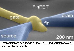
The Delft researchers used an advanced industrial transistor (a MOSFET), which was made as a prototype by IMEC, a research centre in Leuven, Belgium. In this transistor, which consists of approximately 35 nanometre-wide silicon nanowires, the electrical current flows through a single dopant atom (in this case, arsenic). The nanowire is connected to a 'gate'; by applying a voltage to the gate, the researchers enable the electrons to flow through the arsenic atom (from the 'source' to the 'drain'). By detailed measurements of the electrical current's behaviour, researchers can observe the remarkable effects.
This research however does not offer an immediate solution to the problems previously mentioned relating to miniaturisation, but it does provide the industry with greater insights into the (quantum mechanical) behaviour of transitions on the nano level. The research conducted at the Kavli Institute of Nanoscience Delft is also extremely interesting from a purely physics point of view. The transistor that was researched not only provided new insights into the atomic physics occurring inside a solid, but this also resembles a structures that is needed to build a certain type of quantum computer. This still purely theoretical computer - the Kane design - is based on dopant atoms in silicon. One of the advantages of using dopants in silicon is that the realization of such a quantum computer can rely on the extremely well developed silicon nanotechnology.

0 Comments:
Post a Comment
<< Home